Department of Physics, National Central University
Condensed Matter Physics Laboratory

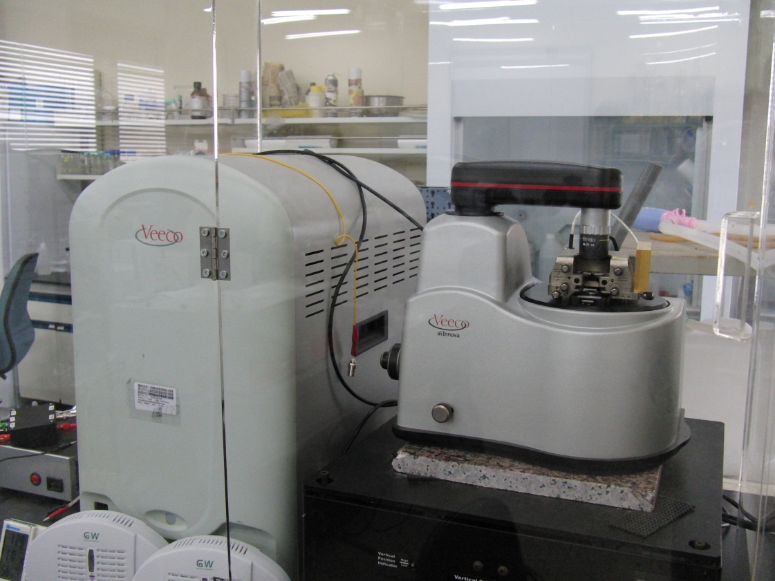
Scanning Capacitance Microscopy
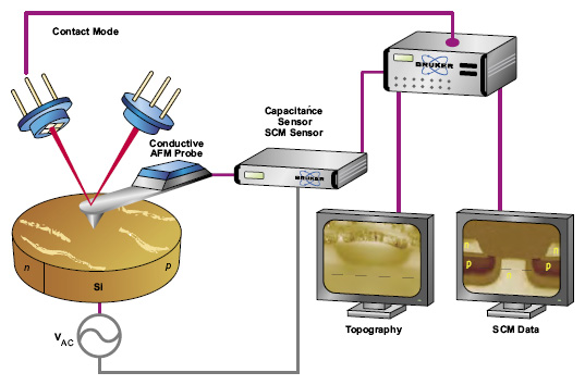
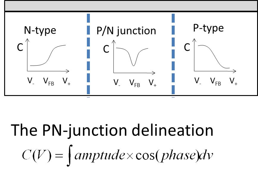
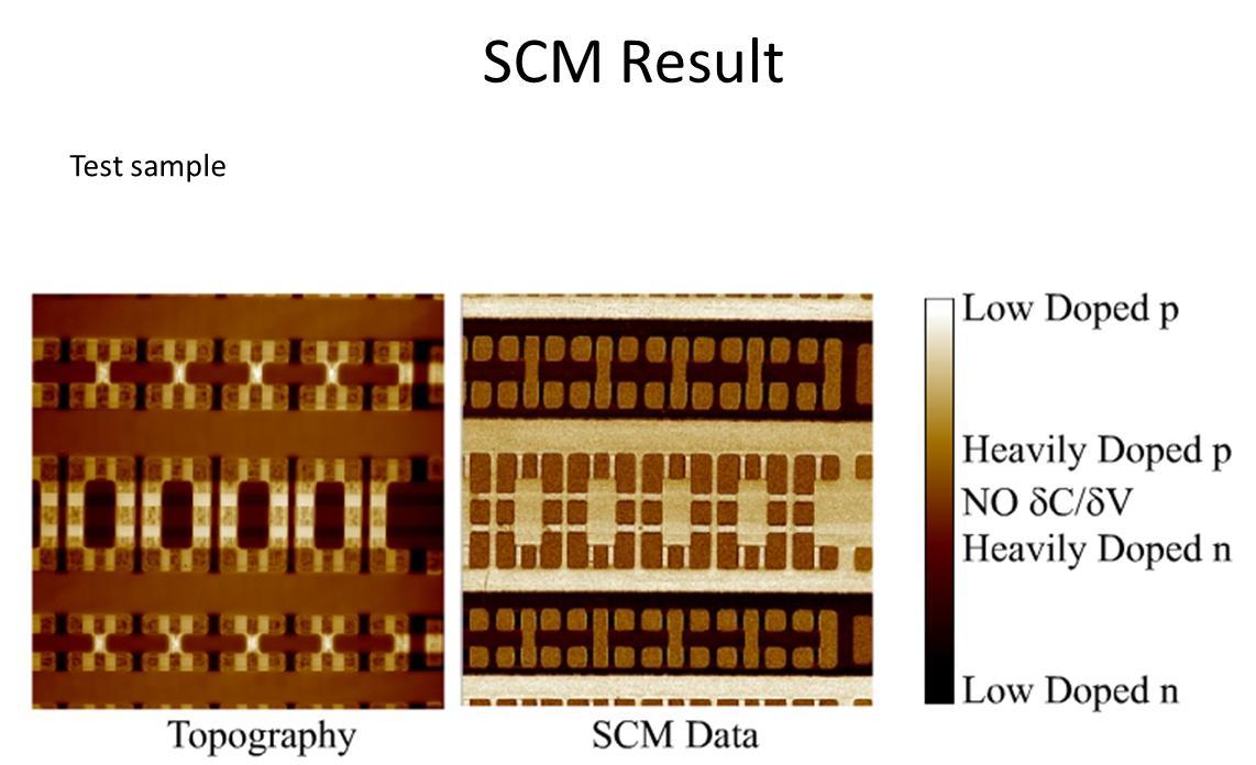
Scanning capacitance microscopy (SCM) is one of the extended operation modes of atom force microscopy (AFM). The main purpose of SCM is to detect the majority carrier type and relative concentration inside the material. This technique is widely used in semiconductor failure analysis.
Basic working principle
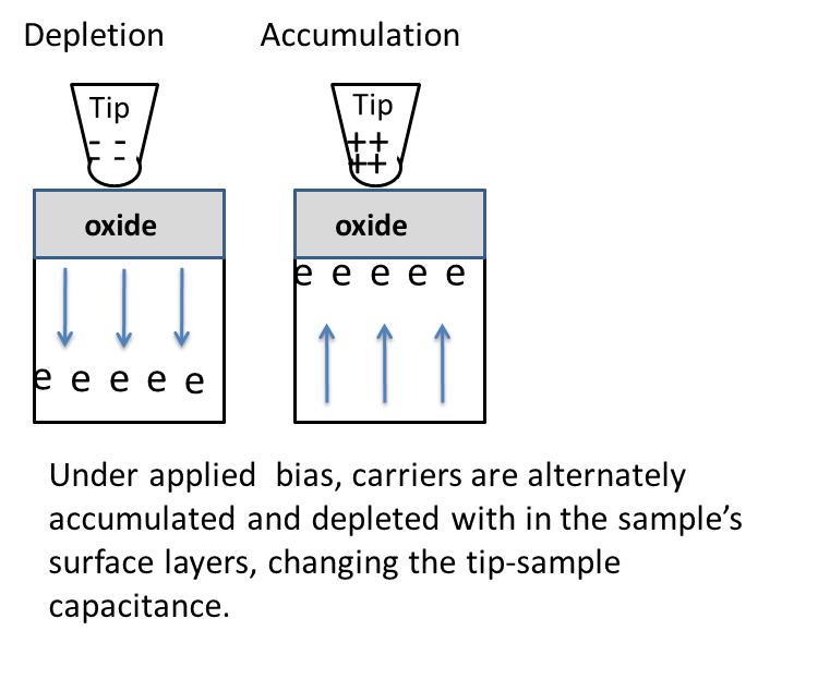
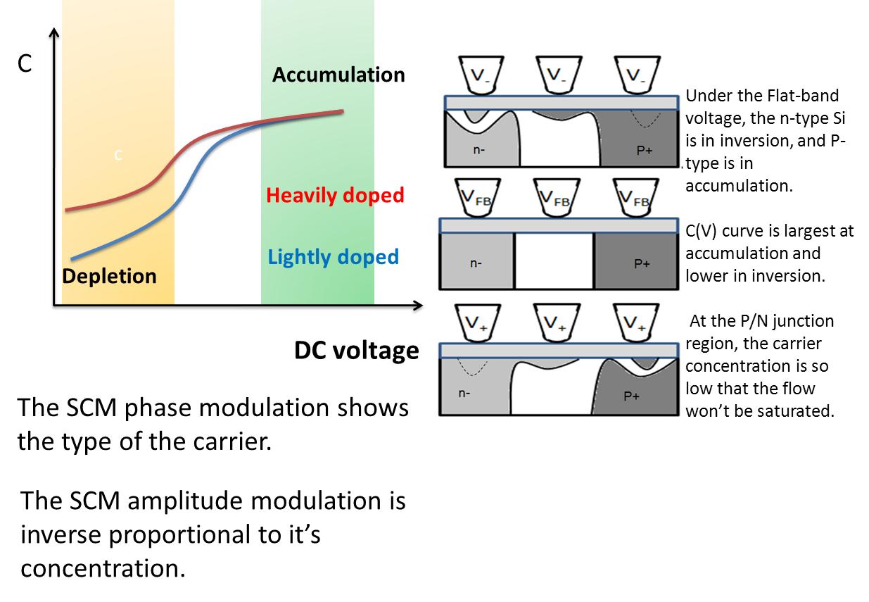
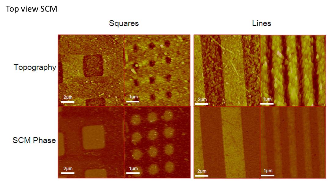
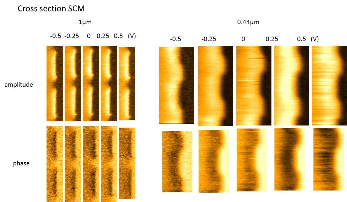
In SCM measurement, a conductive tip is brought to in contact with the sample surface to form a metal-insulator-semiconductor (MOS) interface. As an applied AC electric field is applied, capacitance variation is generated at the surface and can be detected by resonant capacitance sensor. The tip then scans across the sample and give both topography and 2D capacitance profiling at the same time. The benefit of SCM is that the topography and 2D capacitance information do not mix at the same detected signal. Under the applied driving AC field, carriers are alternately accumulated and depleted at the surface, thus changing the MOS capacitance. The feedback carrier motion can be considered as a simple harmonic oscillator. The magnitude and the phase of the capacitance give the information of the majority carrier type and its relative concentration.
© 中央大學凝態物理實驗室 Condensed Matter Physics Laboratory, National Central University
320 桃園縣中壢市中大路300號 No.300, Jhongda Rd., Jhongli City, Taoyuan County 32001, Taiwan(R.O.C.)
Tel: 886-3-4227151ext.65399 | Email: wywoon@phy.ncu.edu.tw